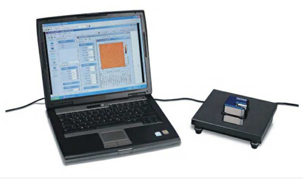
Atomic Resolution of the graphite surface by STM (Scanning Tunneling Microscope)

Approaching a very sharp metal tip to an electrically conductive sample by applying a electrical field leads to a current between tip and sample without any mechanical contact. This so-called tunneling current is used to investigate the electronic topography on the sub nanometer scale of a fresh prepared graphite (HOPG) surface. By scanning the tip line by line across the surface graphite atoms and the hexagonal structure are imaged.
- Observe atoms within minutes
- Custom-designed for use in teaching labs
- Microscope consists of one compact, portable instrument, no additional instruments required
- Vibration-isolated for better and reproducible results
- Can be used both for imaging of atomic resolution and for spectroscopy
- Additional experiment with gold sample can be performed
- With interactive teaching and learning software
Software included. Computer not provided.
Compact STM, Scanning Tunneling Microscope
Graphite model, 2D
Crystal lattice kit: graphite
- Prepare a Pt-Ir tip and the graphite (HOPG) sample and approach the tip to the sample.
- Investigate the topography of clean terraces and the step height between neighboring terraces in constant-current mode.
- Image the arrangement of graphite atoms on a clean terrace by optimizing tunneling and scanning parameters. Interpret the structure by analyzing angles and distances between atoms and atomic rows and by using the 2D and 3D graphite model.
- Measure and compare images in the constant-height and constant-current modes.
- Tunneling effect
- Hexagonal structures
- Scanning Tunneling Microscopy (STM)
- Imaging on the sub nanometer scale
- Piezo-electric devices
- Local Density Of States (LDOS)
- Constant-Height-Mode
- Constant-Current-Mode
